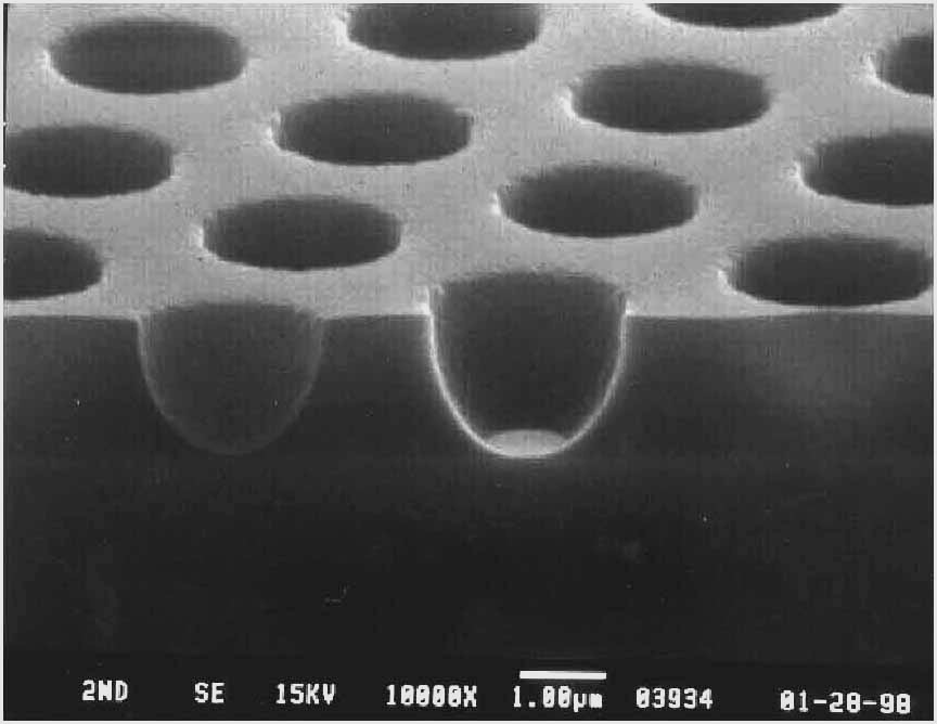
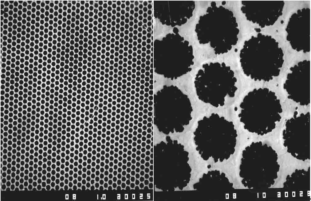
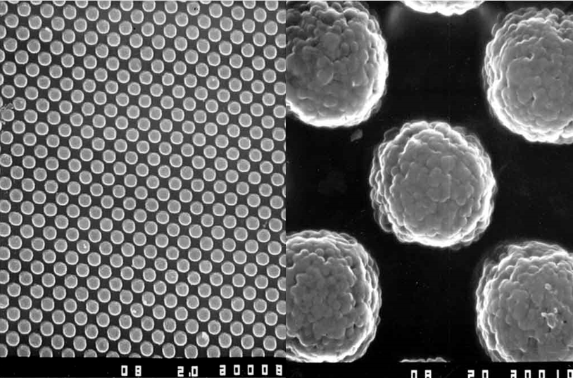
The ability to form micro- and nanosized wells with predetermined shapes and layouts is important for controlling the distribution and packing density of coated particles in applications such as biogenomics and plasmonics.
Our donor-to-receiver transfer process offers a powerful method for forming and processing nanostructures on one substrate (the donor) and then transferring the entire, intact structure to another substrate (the receiver). For example, arrays of microbeads, recrystallized particles or entire electronic circuit layers can be transferred from donor to receiver substrate without disrupting the original structure.
How is this useful? Situations often arise where the conditions required to process one part of a structure could damage another part of the structure, so the ability to isolate these processes can be critical. For example, a high temperature chemical vapor deposition may be required for one step of a process, but the final device must be on a flexible (low temperature) substrate, such as PET or polycarbonate. With our transfer process, the high temperature process could be carried out on a metal foil, glass or wafer (donor) substrate, and the finished structure transferred to the desired final substrate (receiver). Other situations that may require process isolation include wet chemical etching (exposure to strong acids or bases), electroplating (reactive baths), solvent processing (polymer softening or dissolution), high-energy RF plasma processing (damaging electric fields), and vacuum coating (outgassing).
Benefits of Arraying & Transferring
Applications for Arraying & Transferring

Enhanced Photovoltaic Devices

Genomics

Flexible Electronics

Security Films

3D Metamaterials
Work with us to research, develop and launch your project!


