The expanding field of imprinted electronics now includes touch screens, memory devices, health sensors, solid-state lighting films and, most recently, bendable phones. For many of these applications, roll-to-roll manufacturing is often cited as the “holy grail” for low-cost, high-volume manufacturing of components for flexible or rigid applications. However, the current graphic arts printing processes for “printed electronics” have a number of limitations:
- inability to produce lines below tens of microns wide
- limited metallic ink choices for forming circuits
- required high temperature post-processing of conductive inks is incompatible with many common substrates
- printed line conductivity is inferior to that of thin-film metals
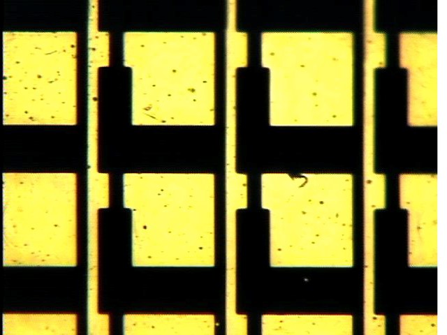
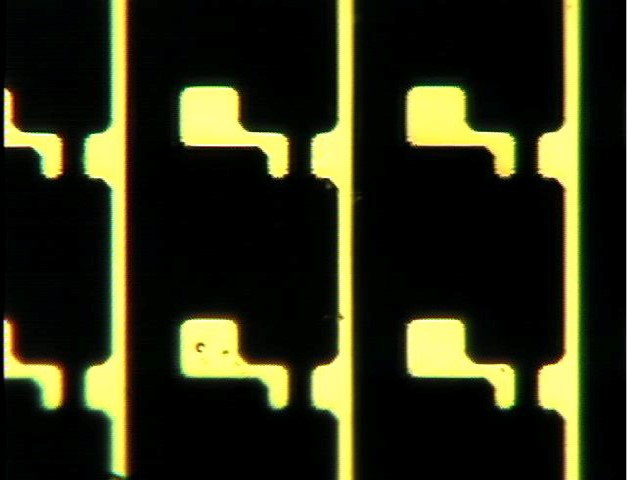
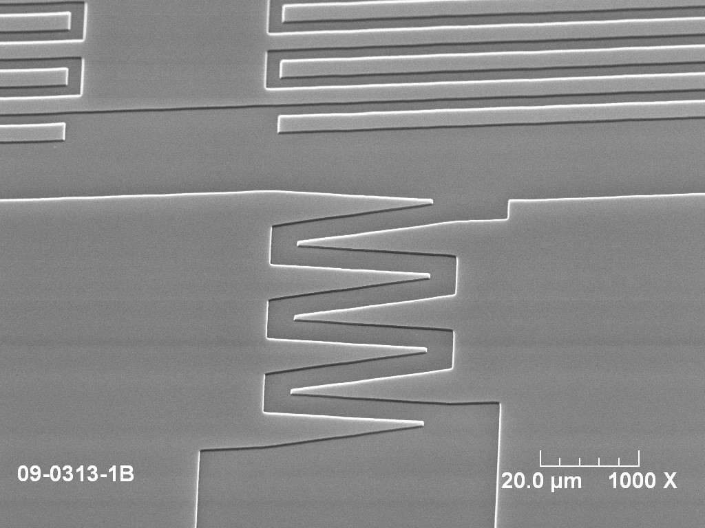
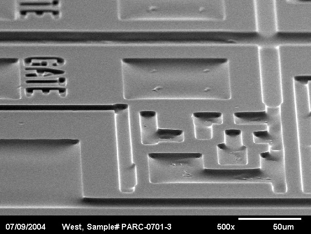
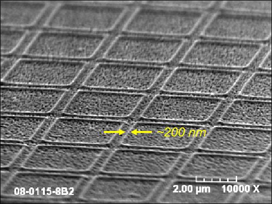
Our optical photomask imprint-patterning process overcomes these limitations to produce highly conductive features, with widths ranging from multi microns down to submicrons, while enabling use of many metals conductors, dielectrics and substrates. This enables denser and higher performance circuitry, and more lightweight, thinner and bendable devices.
Benefits of Our Imprinted Electronics Process
Applications of Imprinted Electronic Circuits

Electronic Sensors

Touchscreen Displays

Light Guiding Films

Light Trapping Film

Transparent Conductors

Thin-Film Optics
Work with us to research, develop and launch your flexible electronic project!