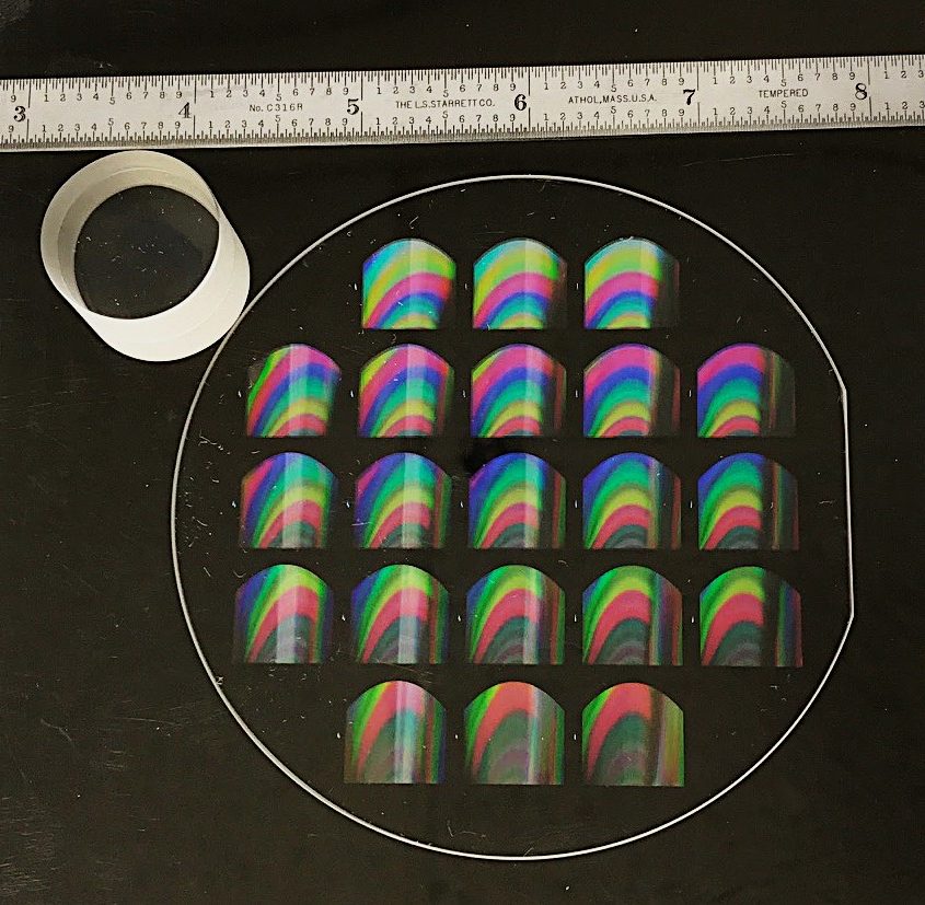
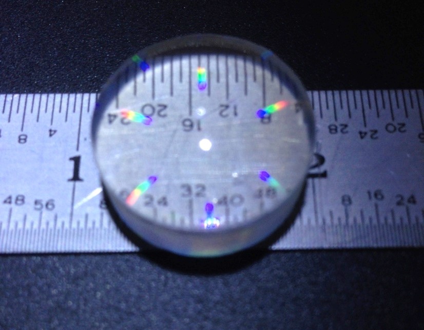
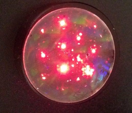
Our patterning processes are not limited to planar or smooth surfaces–they can be applied to non-flat substrates, from cylindrical to complex curved lenses. Using our nanopatterning technology, 3D nano/microstructures, metal mesh and even electronic circuit patterns can be formed on lenses, domes and tubes (inside and out) for improving performance of optics (binary aberration corrections, anti-reflection surfaces), head-up displays, curved touch screens, smart glasses, sensors and more.
Benefits of Our Nanopatterning Technology
Applications for Patterned Curved Surfaces

Anti-reflective Optics, Lenses, Tubes, Domes

Compact, High-Performance Optics

Curved Displays & Touchscreens

Smart Lens
Work with us to research, develop and launch your project!