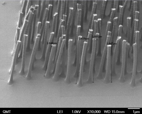
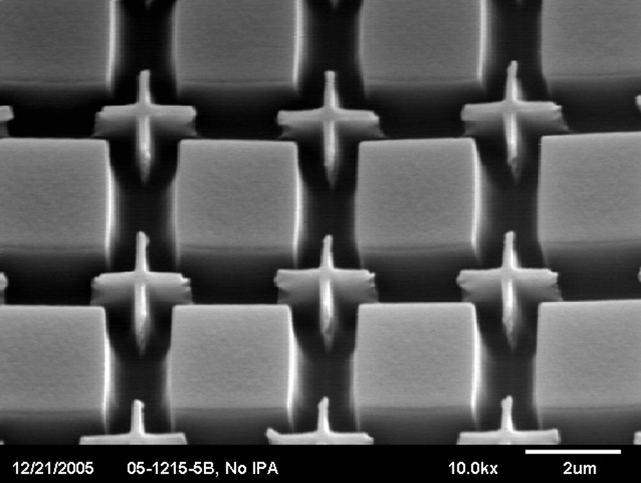
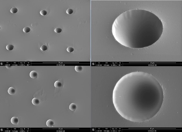
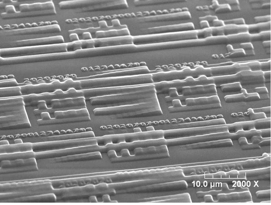
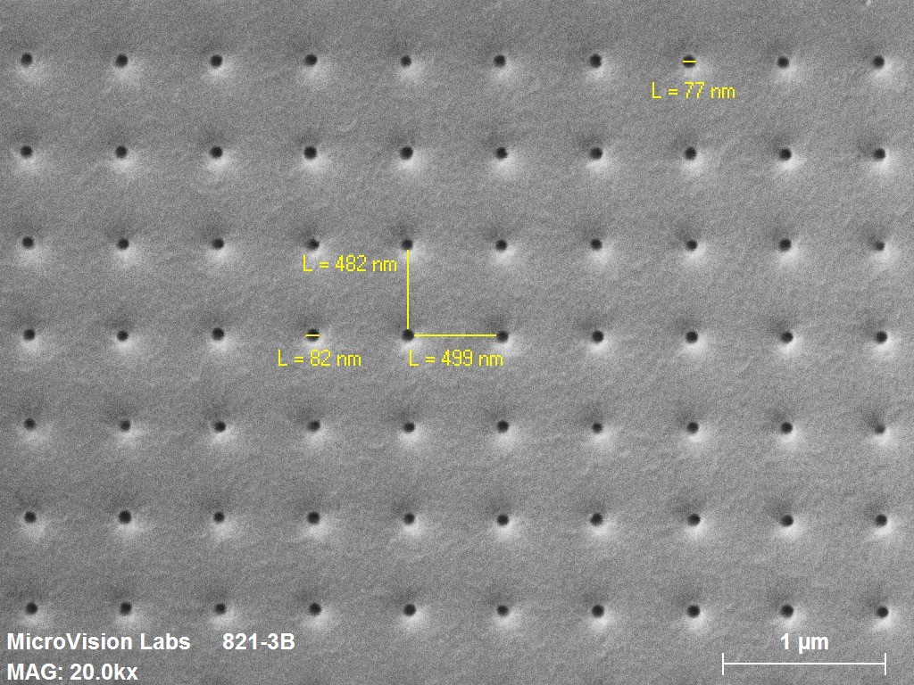
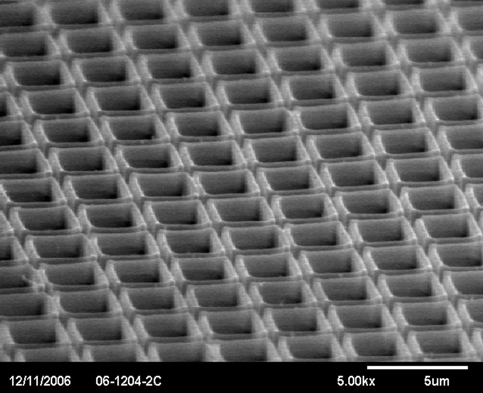
Our proprietary Advanced Surface Nanoforming (ASN™) process creates precise patterns with features in sizes ranging from tens of microns down to tens of nanometers directly into a substrate’s surface. Substrates include polycarbonate, Zeonor and Topas cyclic olefins, PMMA (acrylic), CAB/CAP (cellulose acetates), and more. Because of its reduced temperature processing requirements, ASN eliminates thermal substrate distortion and temperature cycling of patterning templates typical of thermal imprinting. And unlike UV nanoimprinting, ASN also eliminates potential delamination and radiation source issues. Because there is no substrate-polymer interface, adhesion failure and refractive index mismatching are eliminated.
ASN patterning is the process of choice for creating micron to nanometer size structures when failure-proof adhesion is required, whether on thin or thick substrates, when elevated temperatures must be avoided, or for applications requiring the ultimate in optical clarity.
Benefits of Advanced Surface Nanoforming
Applications of Advanced Surface Nanoforming

Diffractive/Binary Optical Elements

Light-Guide Films

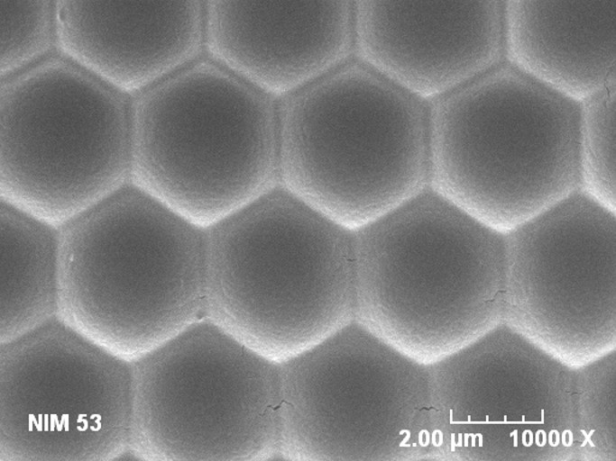
Single or Double-Sided Motheye A/R Films

OLED Light Extraction Substrates

Waveguide Polarizers
Need a micropattern for a custom application? Contact us today to get started.